ultraQUTE: ultrafast QUantum THz nanoElectronicsultraQUTE
Lab

Facilities

The laboratory, equipment and shared facilities behind our THz and quantum nanoelectronics experiments.

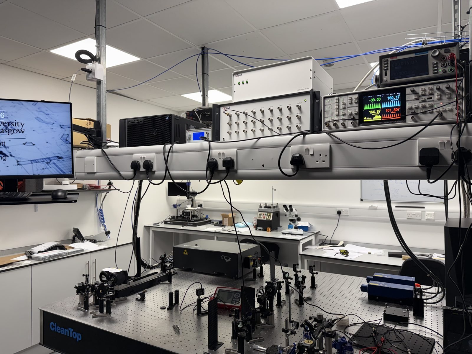
Photo to add: images/facilities/lab-overview.jpgThe UltraQUTE laboratory: optical table with the femtosecond laser and optics, measurement electronics on the shelf above, and workbenches behind

The UltraQUTE laboratory

Our laboratory is in the Rankine Building at the University of Glasgow. It is equipped for THz optoelectronics in both pulsed and continuous-wave mode, and for cryogenic measurements of optoelectronic and nanoelectronic devices.

Alongside the measurement setups we can stack and transfer 2D materials and package chips with optical fibres, so a device can go from fabrication to a fibre-coupled, wire-bonded sample at low temperature within the group.

We are always glad to hear from groups whose work could make use of these capabilities.

Equipment

Photo to add: images/facilities/montana-cryoadvance-100.jpgMontana Instruments CryoAdvance 100 optical cryostat on the optical table, with its sample chamber and touchscreen controller
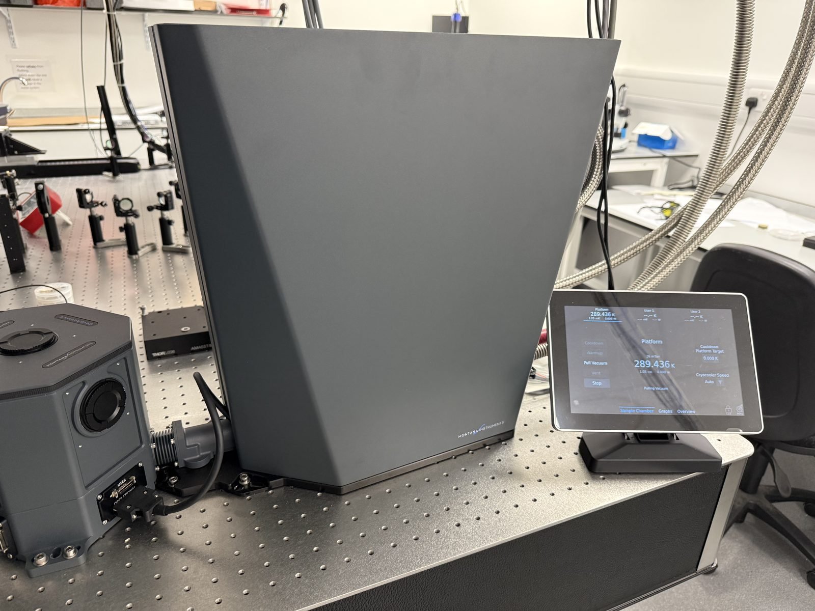
Montana Instruments CryoAdvance 100

Closed-cycle optical cryostat

A cryogen-free optical cryostat that cools samples to about 4 K at the push of a button, with no liquid helium. It has optical ports on the sides and top, so laser beams can reach our opto-electronic device chips while it is cold, and its low vibration suits focused-beam experiments. We use it to operate quantum nanoelectronic devices together with their on-chip THz optoelectronics.

  • Temperature range 3.4 K to 350 K
  • 100 mm diameter sample space
  • 5 optical ports (4 radial, 1 overhead)
  • 75 DC and 4 RF electrical feedthroughs
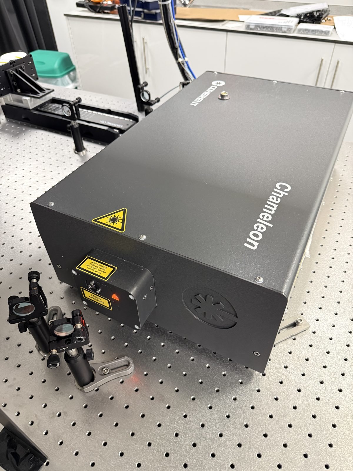
Photo to add: images/facilities/coherent-chameleon.jpgCoherent Chameleon Ultra II femtosecond laser on the optical table

Coherent Chameleon Ultra II

Tunable femtosecond Ti:sapphire laser

The Coherent Chameleon Ultra II: A wavelength-tunable Ti:sapphire oscillator that delivers 100 femtosecond pulses in the spectral range of 680nm to 1080nm. Its pulses trigger our photoconductive switches to generate and sample picosecond electrical pulses, in pump-probe measurements with sub-picosecond timing.

  • 100 fs pulses
  • Tunable from 680 nm to 1080 nm
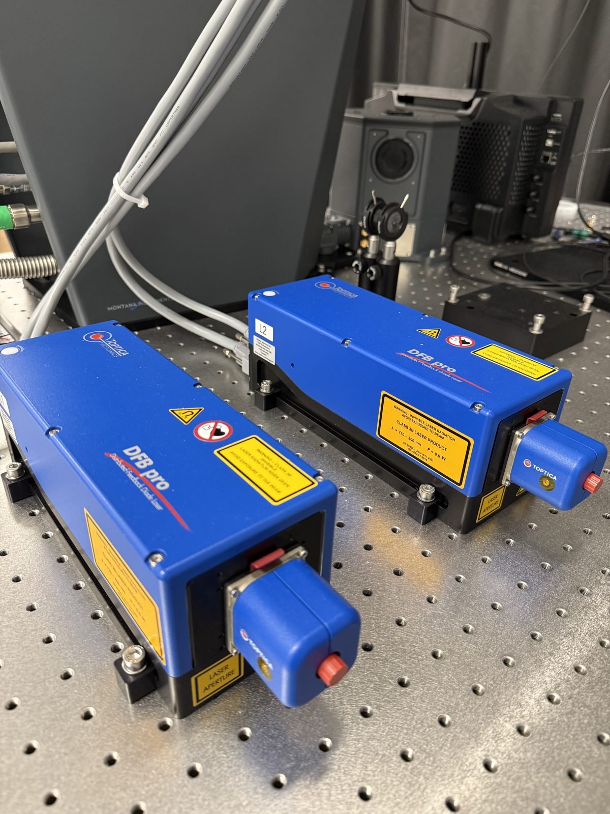
Photo to add: images/facilities/toptica-dfb-pro.jpgTwo TOPTICA DFB pro diode lasers on the optical table, used for continuous-wave THz generation

TOPTICA DFB pro

Continuous-wave THz generation by photomixing

A pair of distributed-feedback diode lasers at 800 nm whose difference frequency is converted into continuous-wave THz radiation in our photo-conductive switches. Tuning one laser against the other sweeps the THz frequency continuously, which gives narrow-linewidth, frequency-resolved THz measurements that complement our pulsed, time-domain experiments.

  • Continuous-wave, tunable THz output
  • Laser wavelength 800 nm
  • Fine frequency steps
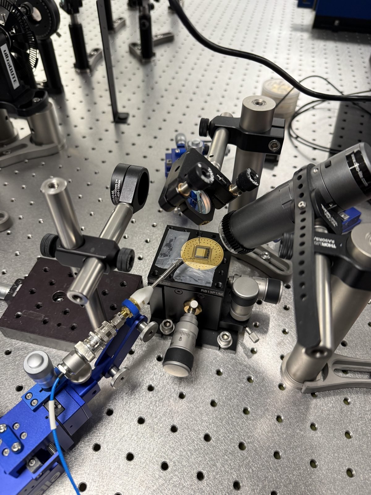
Photo to add: images/facilities/chip-characterisation.jpgA picosecond-pulse generation chip mounted on a gold PCB under test on the optical table, with a probe and focusing optics

Optoelectronic chip characterisation

Testing picosecond-pulse chips on their PCBs

A typical setup for characterising a picosecond-pulse generation chip and its PCB on the optical table, before the device is cooled down.

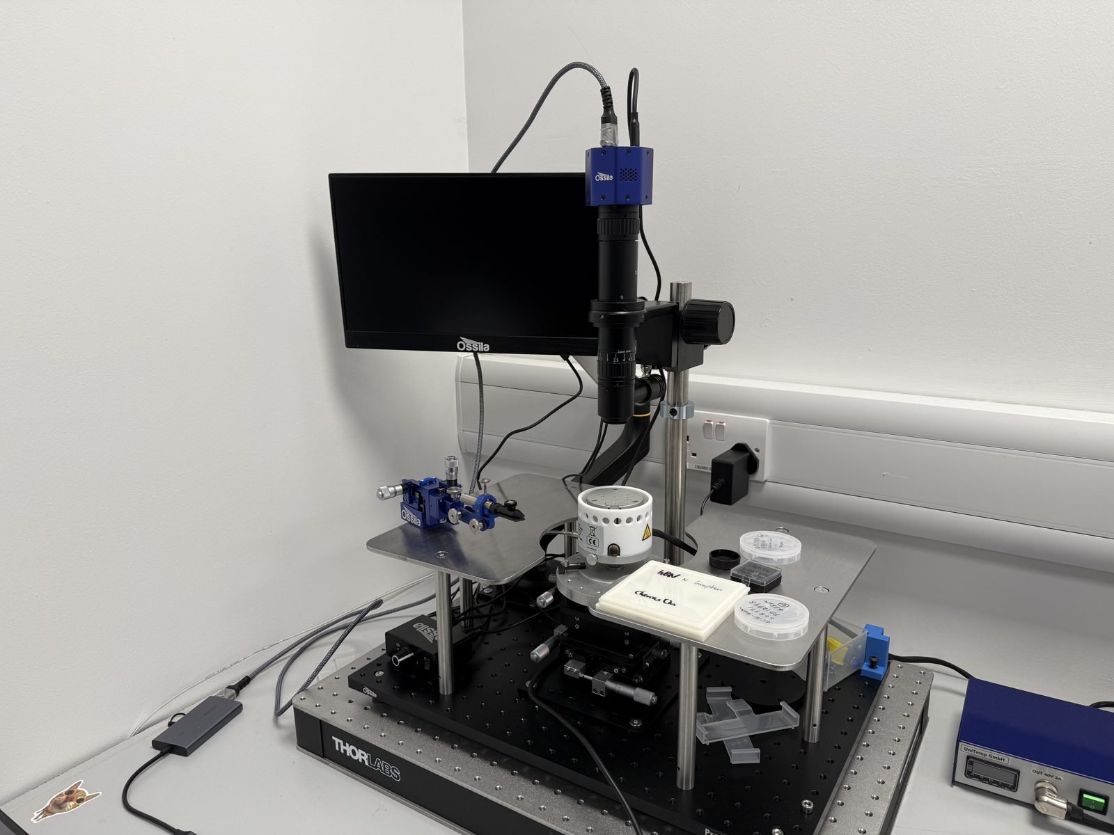
Photo to add: images/facilities/2d-transfer-station.jpg2D material transfer station with microscope camera, heated stage and micromanipulator

2D material transfer station

Assembly of van der Waals heterostructures

Used to stack two-dimensional materials on top of one another with micrometre alignment, for example hBN-graphene-hBN heterostructures.

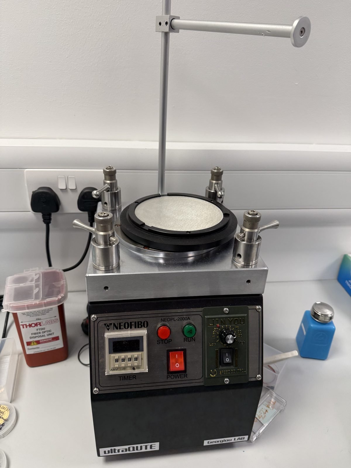
Photo to add: images/facilities/fibre-polishing-machine.jpgFibre polishing machine with its polishing plate and fibre holder posts

Fibre polishing machine

Custom fibre connectors and chip-to-fibre packaging

Used to fit optical fibres with custom connectors and to package our optoelectronic THz photoconductive switches with fibres.

Manufacturing scientific instrumentation

We design and build our own measurement electronics, so that each instrument matches the needs of our low-temperature and THz experiments. This includes low-noise transimpedance amplifiers, voltage amplifiers, low-noise digital-to-analogue converters (DACs), source meters and data-acquisition electronics.

More details of our instruments will be added here.

Shared facilities

James Watt Nanofabrication Centre (JWNC)

The University of Glasgow's open-access nanofabrication facility, where our devices are made. It supports semiconductors, quantum technologies, photonics and advanced electronics, from early-stage research and prototyping through to low-volume manufacture.

  • Electron-beam lithography down to 5 nm, with sub-nanometre layer-to-layer alignment
  • UV photolithography and nanoimprint lithography
  • Electron-beam evaporation of metals, including Al, Au, Ti, Pt and Ge
  • Plasma etching (ICP, RIE, deep silicon etch), PECVD and ALD
  • Metrology: SEM with EDX, AFM and ellipsometry

JWNC website

Centre for Advanced Electronics (CAE)

A centre in the James Watt School of Engineering, established in 2006, for designing, modelling and testing nanoelectronic, power, high-frequency and flexible electronic devices.

  • On-wafer network analysis from 10 MHz to 110 GHz and from 140 GHz to 325 GHz
  • Free-space and material characterisation from 750 GHz to 1.1 THz
  • Cryogenic and temperature-controlled probe stations, from 77 K
  • Semiconductor device analysers for DC and pulsed I-V and C-V
  • 50 GHz oscilloscope and arbitrary waveform generation up to 70 GHz
  • Antenna measurement, including an anechoic chamber and near-field scanning up to 325 GHz

CAE website

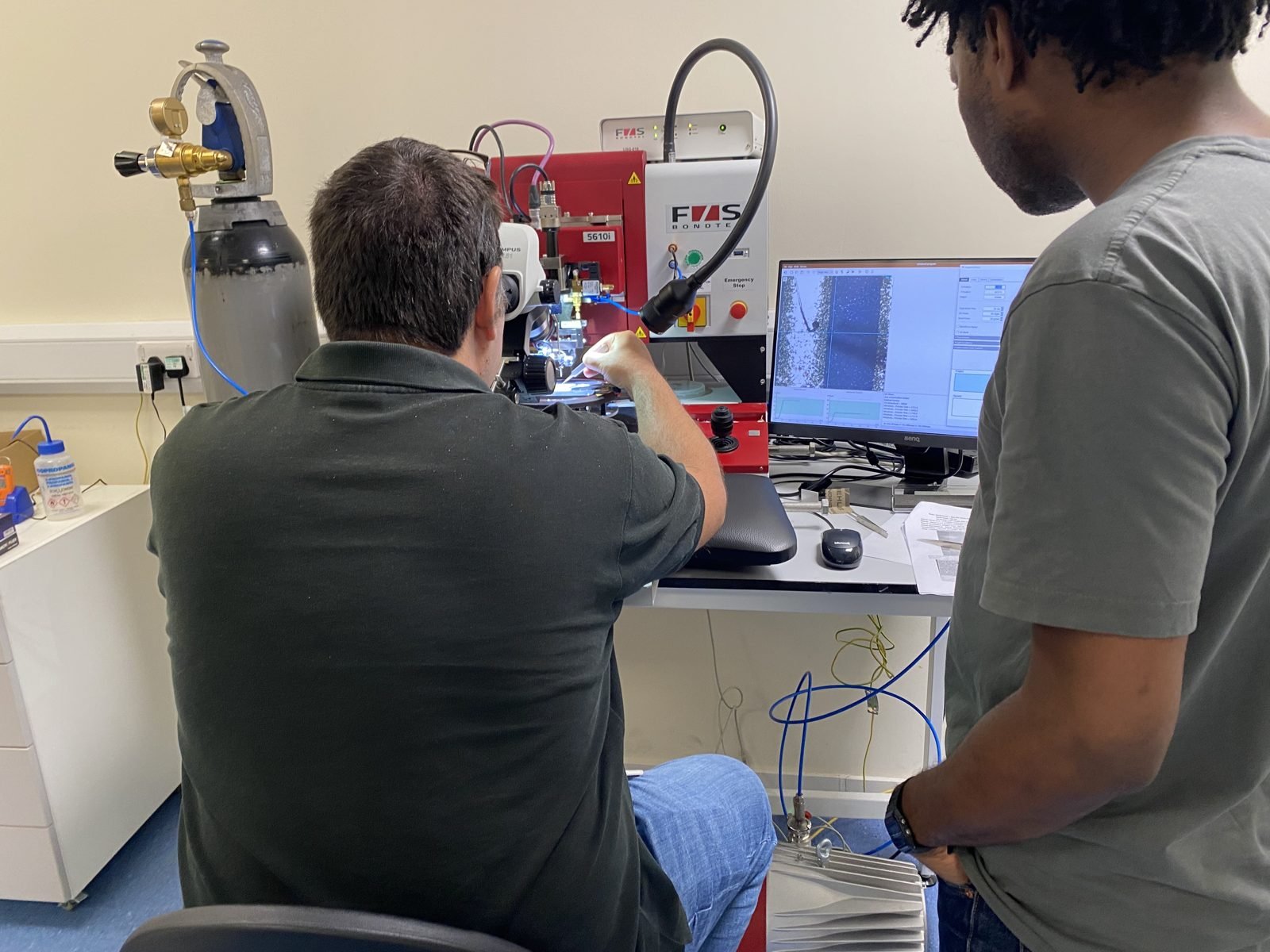
PhotoTwo group members wire bonding a device on the F&S Bondtec 5610i ball-wedge bonder

F&S Bondtec 5610i wire bonder

A semi-automatic ball-wedge bonder with a microscope and camera view, used to connect the bond pads of our chips to our homemade PCBs with fine wires before the device goes into the cryostat. Our devices, bonded to our PCBs, can contain up to 100 connections.